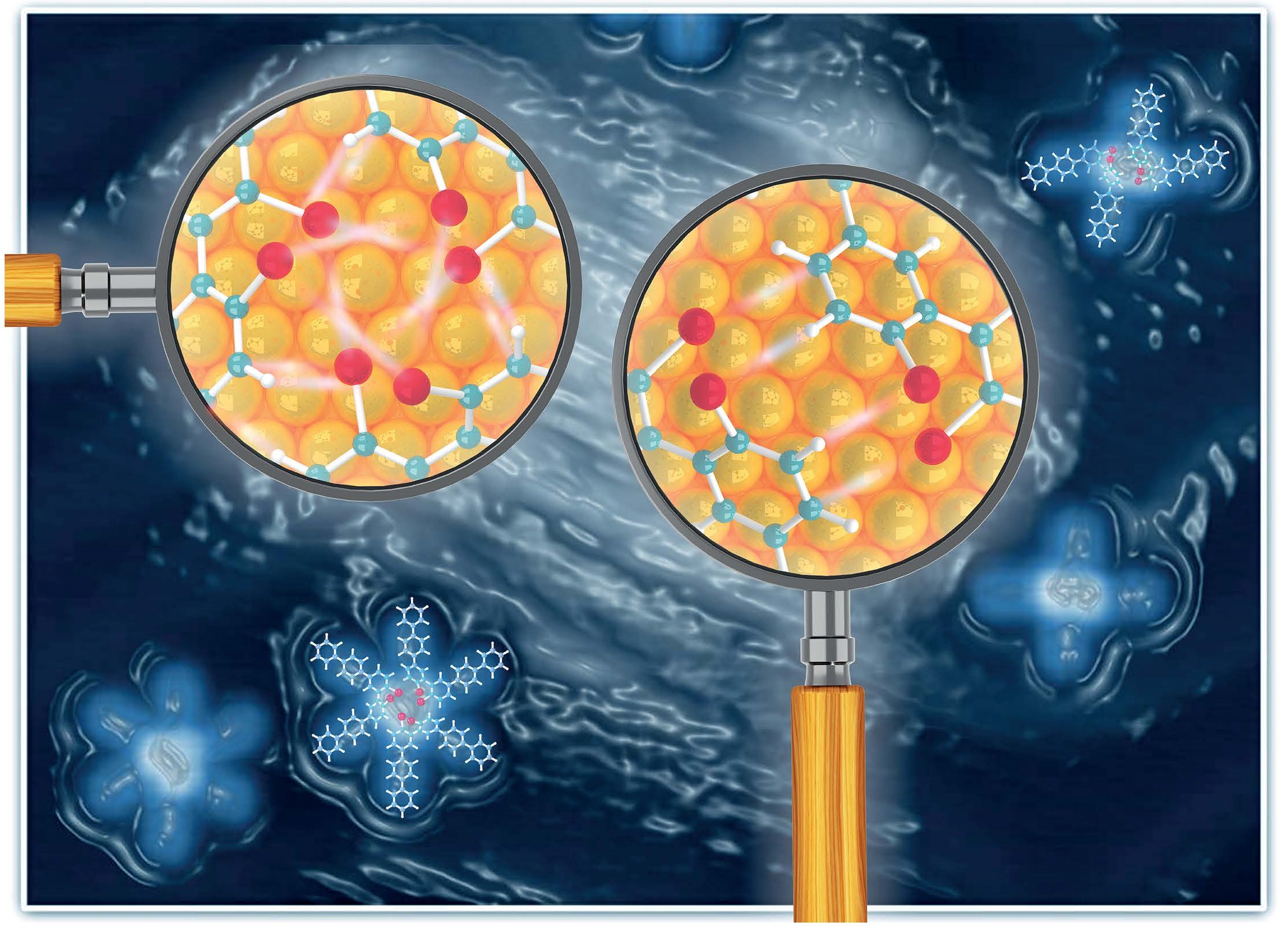
Non-covalent interactions govern many chemical and biological processes, crucial for the design of drugs and controlling molecular assemblies and their chemical transformations. However, atomic-scale real-space characterization of these weak interactions in complex molecular architectures has been challenging. Here, we employed bond-resolved scanning probe microscopy combined with an exhaustive structural search algorithm and quantum chemistry calculations to elucidate multiple non-covalent interactions that control the cohesive molecular clustering of well-designed precursor molecules and their chemical reactions. This work is published in Chemical Science , selected as ChemSciPicks, with cover art image.
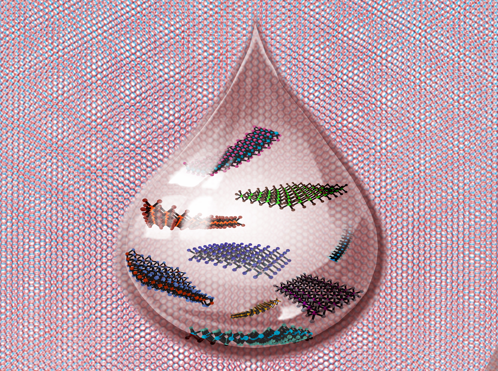
Highly crystalline 2-D transition metal dichalcogenide superconductors and their associated (van der Waals) heterostructures provide a rich platform for the investigation of new quantum physics and exotic superconductivity. Here we have developed a universal electrochemical exfoliation method for the synthesis of highly-crystalline, two-dimensional superconducting monolayers (2DSC). These 2DSC monolayers are obtained in a stable suspension with monolayer production yield of up to 75%. They can be used for fabricating artificially designed structures that exhibit superconducting properties. This includes printing wafer-level 2-D superconducting wires and constructing superconducting composites using 3-D printing techniques. This work is published in Nature Materials, Highlighted in Phys.org, Nanowerk, Azo Nano, News Break, and FOS Science.
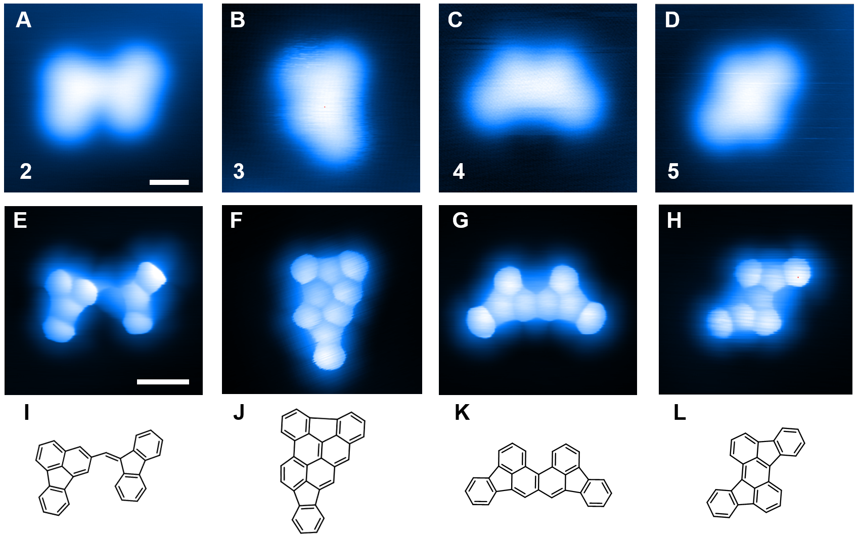
Imaging a radical reaction
Bond-resolved scanning tunneling microscopy unambiguously resolves various products formed through a complex structural dissociation and rearrangement of organic monoradicals. Our study provides unprecedented insights into complex surface reaction mechanisms of organic radical reactions at the single molecule level, which may guide the design of stable organic radicals for future quantum technology applications.

Strain-induced isomerisation of molecular chains
NUS scientists have demonstrated a strain-induced structural rearrangement of one-dimensional (1D) metal-organic molecular chains for potential use in fabricating functional nanostructures. The synthesis of functional materials at the molecular level can potentially be used to develop nanostructures for applications requiring specially tailored electronic and magnetic properties. This is usually achieved by using thermal- or photo-triggered chemical transformations. The use of mechanical strains to trigger chemical transformations provides a new way to fabricate nanostructures with unique properties. The findings on the strain-induced structural rearrangement in one-dimensional material systems will enrich the available toolbox for on-surface synthesis of novel functional materials and quantum nanostructures. This work is published in Angewandte Chemie, Highlighted in Phys.org, Nanowerk and FOS Science.
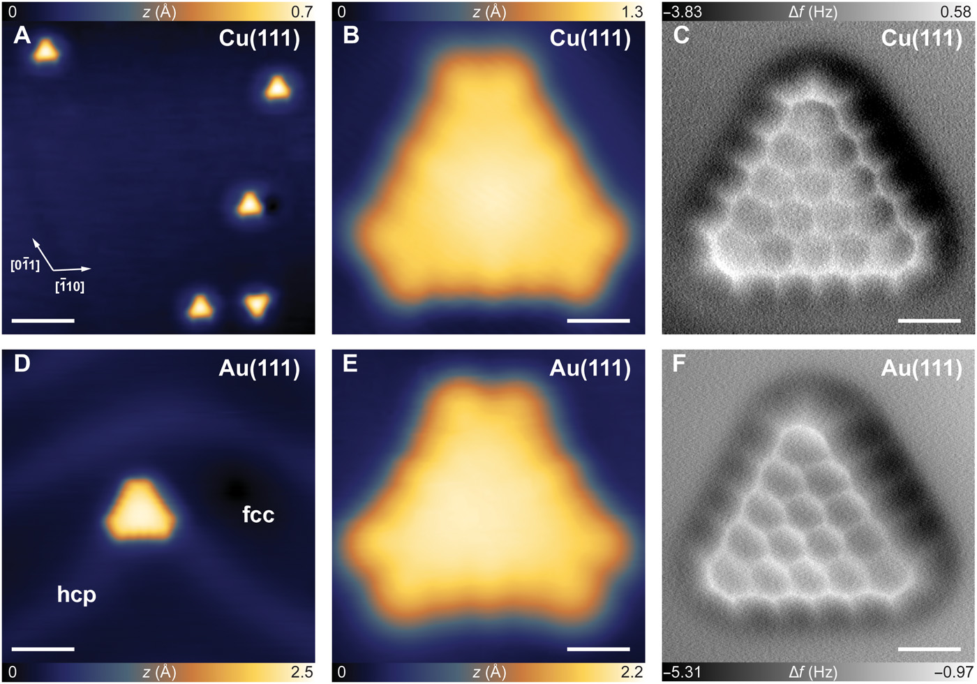
A magic graphene molecule
On-surface synthesis of π-extended triangulene enables the characterization of its spin-polarized edge states. The synthetic process will open a new avenue to engineer larger, triangular zigzag edged graphene quantum dots with atomic precision for spin and quantum transport applications. It is therefore of great interest to continue generating similar systems with diverse sizes and spin numbers to uncover their properties on a variety of substrates using spin-polarized STM studies. This work is published in Science Advances, Highlighted in Phys.org.
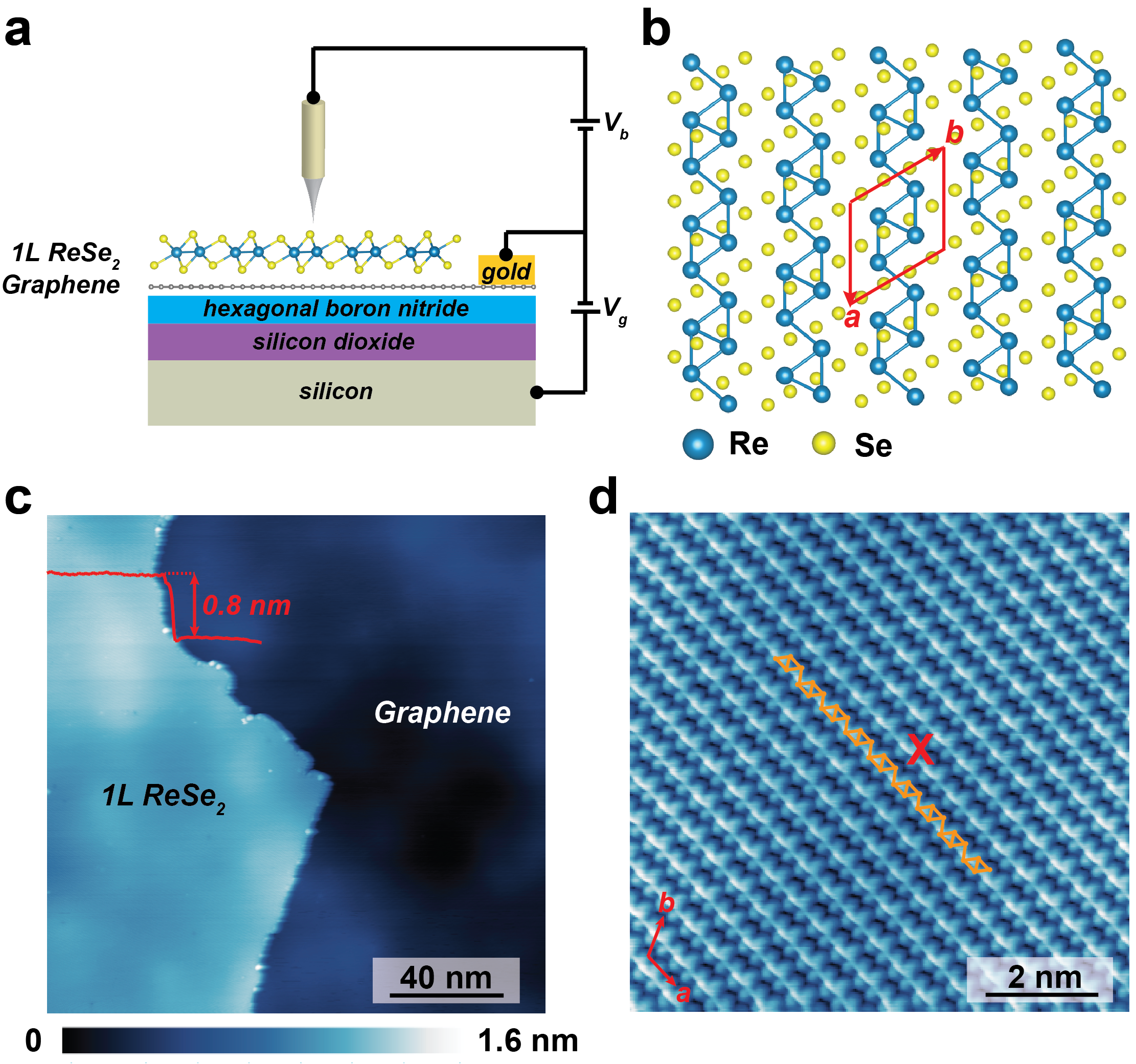
Remote control of excitons in a 2D semiconductor
Remote control of excitons in a two-dimensional semiconductor is achieved by tuning electron density in adjacent graphene. The results showed that screening from a graphene substrate had profound impact on Coulomb interactions that lead to broad tunability of the electronic band gap and exciton binding energy. The findings revealed many-electron physics in hybrid 2D semiconductors or graphene systems. The work will pave the way to control excitonic effects and precisely tune the exciton binding energies in 2D semiconductors for a variety of technical applications. This work is published in Science Advances, highlighted in Phys.org, Azom Materials and Nanowerk.
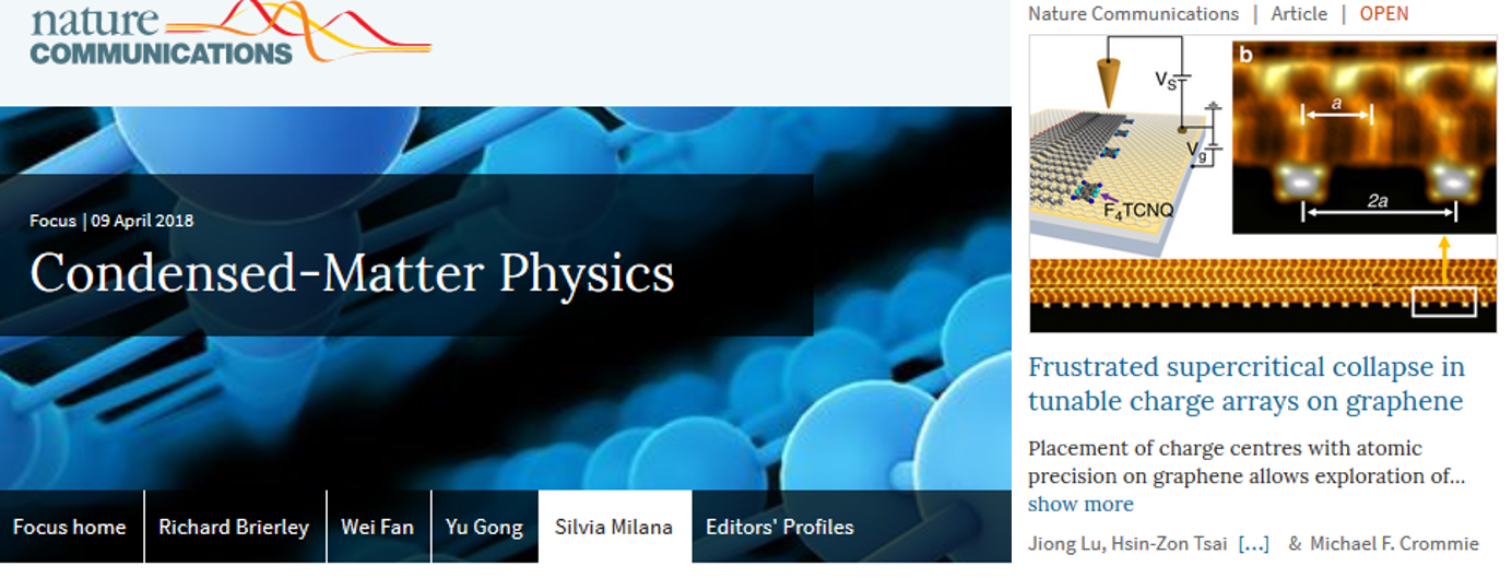
Frustrated supercritical collapse
Placement of charge centres with atomic precision on graphene allows exploration of new types of confinement of charge carriers. Here, the authors fabricate atomically precise arrays of point charges on graphene and observe the onset of a frustrated supercritical regime. This work has been selected as editor choice in Nature Communications 2019
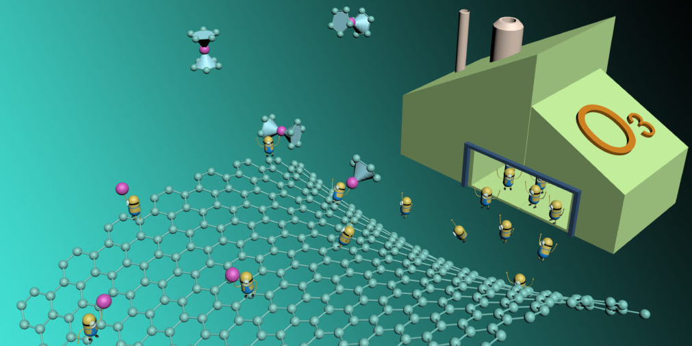
Tuning Single Atom Density with Ozone
Controllable synthesis of single atom catalysts with sufficiently high metal loading remains challenging due to the tendency of agglomeration. Here we synthesize a series of stable atomically dispersed cobalt atoms on graphene with high Co loadings via the regeneration of active sites by atomic layer deposition. This work has been published in Nature Communications 2018. and BEHIND THE PAPER in Nature Research Chemistry Community.
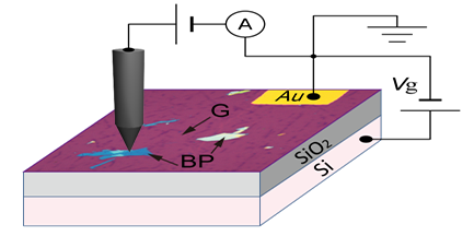
A Large Area Pseudo-Magnetic Field in Graphene on BP
Spatially tailored pseudo-magnetic fields (PMFs) can give rise to pseudo-Landau levels and the valley Hall effect in graphene. At an experimental level, it is highly challenging to create the specific strain texture that can generate PMFs over large areas. Here, we report that superposing graphene on multilayer black phosphorus creates shear-strained superlattices that generate a PMF over an entire graphene–black phosphorus heterostructure with edge size of tens of micrometres. The PMF is intertwined with the spatial period of the moiré pattern, and its spatial distribution and intensity can be modified by changing the relative orientation of the two materials. This work has been published in Nature Nanotechnology 2018, See the highlight in Phys.org here
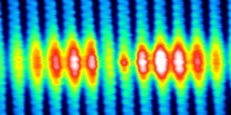
Bound Hole States in Black Phosphorous
A team led by Prof LU Jiong has discovered that when BP goes from a non-excited ground state to an excited state, the spatial shape of its bound hole states evolves from an extended elliptical shape to a dumbbell shape. In BP, each hole interacts and orbits around the negatively charged core, forming bound hole states. This is analogous to the Bohr model for the hydrogen atom, in which the single electron encircles the atomic nucleus. Their findings provide a generic picture of the spatial structure and electronic properties of bound states near shallow dopants in BP. This work has been published in Nano Letters 2017, See the highlight in Phys.org here
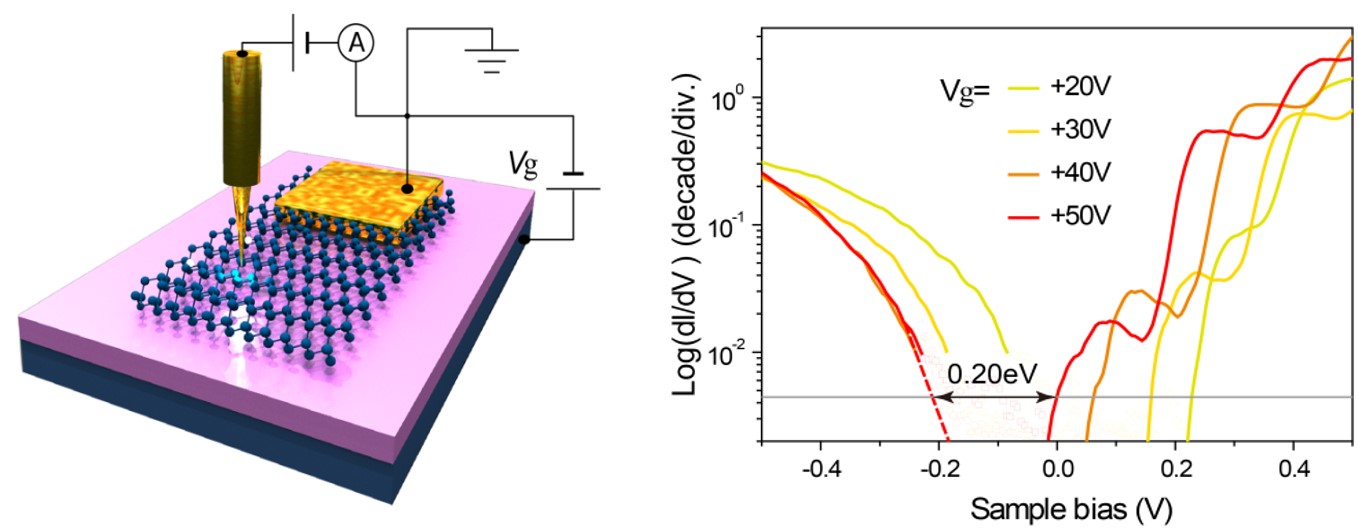
Giant Stark effect in Black Phosphorus
BP is one of the few two-dimensional (2D) materials where it is possible to tune the bandgap over a wide energy range from the visible to the IR spectrum. Although theoretical computations have predicted that the electrical and optical properties of ultrathin BP can be effectively tuned by electrostatic doping, it has not been physically demonstrated. This is due to difficulties in the preparation of 2D BP devices and its high reactivity when exposed to air which has so far limited experimental investigations. Prof Lu and his team has achieved a notable bandgap reduction of ~35.5% (from 0.31 eV to 0.2 eV) by applying a vertical electric field of 0.1 V/nm. This work has been published in Nano Letters 2017, See the highlight in Nature Photonics.

